Syllabus
Fundamentals of Digital Design
1.1 Review of basic gates, Universal gates, Minimization of logical expressions with Boolean Algebra
1.2 Review of Number system and coding techniques.
1.3 Combinational logic representation using truth table, sum of products(SOP) and products of sum(POS), Minimization of logical expressions with Karnaugh Map (up to five variables) and realization.
1.4 Quine McCluskey Method for minimization
Combinational Logic Circuits
2.1 Design of different combinational circuits, Adder, subtractor, controlled adder/ subtractor, BCD adder/subtractor, Use of MSI devices
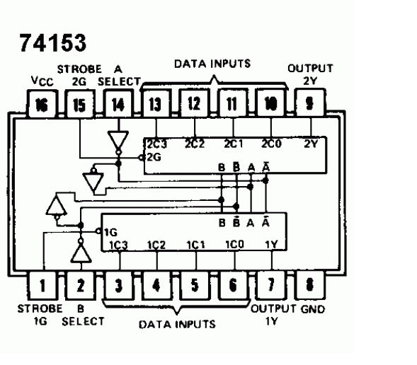
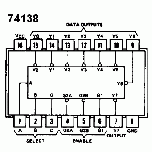
2.2 Multiplexer, demultiplexer, decoder, encoder, comparator, multiplexer tree and decoder tree. Use of MSI devices
2.3 Introduction, realization of logic expressions with PROM, PLA and PAL.
Carry Look ahead adder
Sequential Logic Design
3.1 Latches and flip flops
3.2 Asynchronous counters, synchronous counter, up/down counter, mod counter, shift register
3.3 Design using MSI counters and shift register
Finite State Machines Design
4.1 Mealy and Moore Machines, Clocked synchronous state machine analysis
4.2 Development of state diagram, State reduction techniques and state assignment, Clocked synchronous state machine design.
4.3 Design applications like sequence detectors, vending machines
Logic Families and Programmable Devices
5.1 Introduction to CPLD and FPGA architectures.
5.2 Introduction to HDL
Types of logic families (TTL and CMOS), characteristic parameters (propagation delays, power dissipation, Noise Margin, Fan-out and Fan-in)
1.1 Review of basic gates, Universal gates, Minimization of logical expressions with Boolean Algebra
1.2 Review of Number system and coding techniques.
1.3 Combinational logic representation using truth table, sum of products(SOP) and products of sum(POS), Minimization of logical expressions with Karnaugh Map (up to five variables) and realization.
1.4 Quine McCluskey Method for minimization
Combinational Logic Circuits
2.1 Design of different combinational circuits, Adder, subtractor, controlled adder/ subtractor, BCD adder/subtractor, Use of MSI devices
2.2 Multiplexer, demultiplexer, decoder, encoder, comparator, multiplexer tree and decoder tree. Use of MSI devices
2.3 Introduction, realization of logic expressions with PROM, PLA and PAL.
Carry Look ahead adder
Sequential Logic Design
3.1 Latches and flip flops
3.2 Asynchronous counters, synchronous counter, up/down counter, mod counter, shift register
3.3 Design using MSI counters and shift register
Finite State Machines Design
4.1 Mealy and Moore Machines, Clocked synchronous state machine analysis
4.2 Development of state diagram, State reduction techniques and state assignment, Clocked synchronous state machine design.
4.3 Design applications like sequence detectors, vending machines
Logic Families and Programmable Devices
5.1 Introduction to CPLD and FPGA architectures.
5.2 Introduction to HDL
Types of logic families (TTL and CMOS), characteristic parameters (propagation delays, power dissipation, Noise Margin, Fan-out and Fan-in)
For ISE students should refer to following video lecture course:
https://www.nesoacademy.org/ec/05-digital-electronics
IA2
The student should complete the IA 2 on paper (Handwritten) to Ninad Sir (A-div) and Arati Madam (B-div) on and before 25th Oct 2023
Google Classroom code: g7smowd
https://classroom.google.com/c/NTIzMTc3Mzg5MDY3?cjc=g7smowd
https://classroom.google.com/c/NTIzMTc3Mzg5MDY3?cjc=g7smowd
| DE__writeup_experiment_2.docx |
| DE_writeup_experiment_3_adder_subtractor.docx |
Experiment BCD adder
| DE_writeup_experiment_4_bcd_adder.docx |
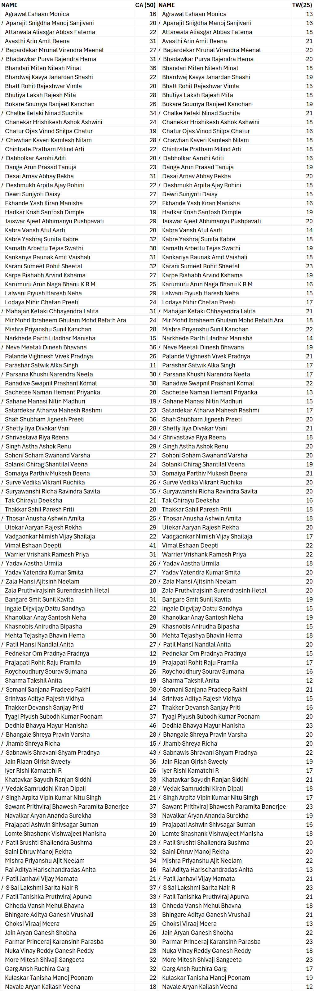
Experiment Multiplexers and Decoders
|
|
|
|
|
|
|
|
|
|
|
|
|
|
|
|
|
|
|
|
|
|
|
|
|
|
|
|
|
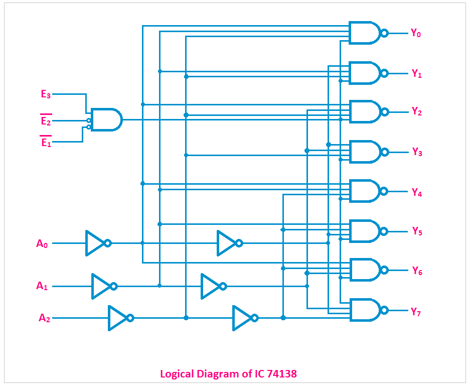
| DE__writeup_experiment_5 MUX and decoder.docx |
Experiment Flipflops
|
|
|
A modulo 6 (MOD-6) counter circuit, known as divide-by-6 counter, can be made using three D-type flip-flops. The circuit design is such that the counter counts from 0 to 5, and then on the 6th count it automatically resets to begin the count again. Since we are using the sixth count itself to cause a reset, it is unstable. The trick is to start with a MOD-8 counter and then look for the binary sequence 110, which is 6 in decimal. Since this binary sequence is unique, we look for the sequence of 1’s and feed them into an AND gate. The output from the AND gate is then used to control the RESET function on all three flip-flops. Remember that binary is read from right to left (LSB to MSB), whilst the counter output is left to right. Students are likely to make mistakes here, and end up using the incorrect outputs to feed the AND gate.
| DE__writeup_experiment_6_ff.docx |
| de__writeup_experiment_7_onwards__1_.docx |
IA 1