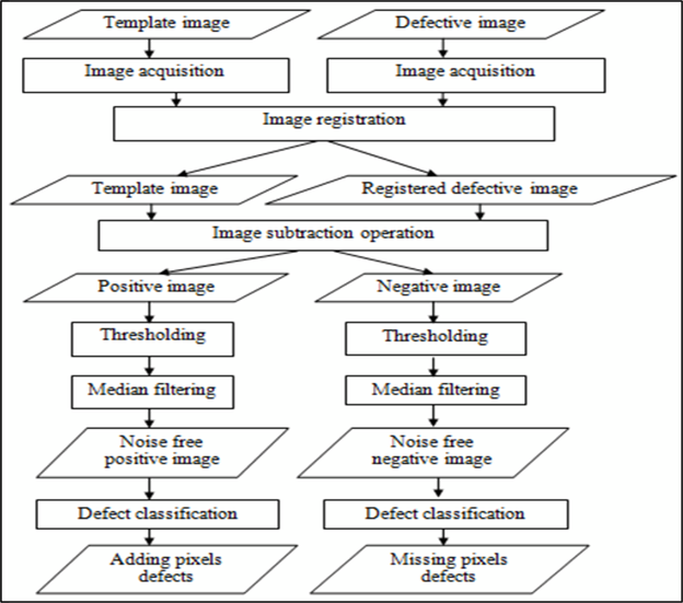
A printed circuit board or (PCB) is used to mechanically support and electrically connect electronic components using conductive pathways, track or signal traces etched from copper sheets laminated onto a conductive substrate. The automatic inspection of PCBs serves a purpose which is traditional in computer technology. The purpose is to relieve human inspectors of the tedious and inefficient task of looking for those defects in PCBs which could lead to electric failure. We first compare a PCB standard image with a PCB image, using a simple subtraction algorithm that can highlight the main problem-regions. We have also seen the effect of noise in a PCB image that at what level this method is suitable to detect the faulty image. Finally, defect classification operation is employed in order to identify the source for six types of defects namely, missing hole, pin hole, under etch, short-circuit, mouse bite, and open-circuit.